[Download 41+] Antenna Effect In Vlsi
Get Images Library Photos and Pictures. Mitigating antenna effect in IC design(3) Special Cells used in VLSI Physical Design Mitigating antenna effect in IC design(2) Detection of an antenna effect in VLSI designs | Semantic Scholar
. Antenna effect - Wikipedia Antenna Effect in 16nm Technology Node PDF) The Antenna Effect: Problem and Solutions | A Đỗ Tấn - Academia.edu

Antenna effect in VLSI Fabrication | Plasma Induced Gate Oxide Damage | Plasma Etching
 Detection of an antenna effect in VLSI designs | Semantic Scholar
 VLSI Backend Design: Antenna Effect
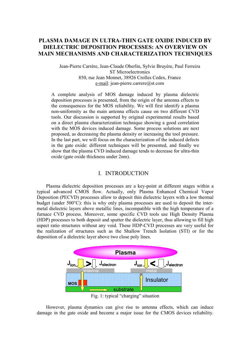 PDF) Plasma Damage in Ultra-Thin Gate Oxide Induced by Dielectric Deposition Processes: An Overview on Main Mechanisms and Characterization Techniques
 Antenna effect in VLSI Fabrication | Plasma Induced Gate Oxide Damage | Plasma Etching - YouTube
 Discharge-path-based antenna effect detection and fixing for X-architecture clock tree - ScienceDirect
 Antenna effect in VLSI
 Vlsi
Vlsi
 Team VLSI: Antenna Prevention Techniques in VLSI Design
 Antenna Effects |VLSI Concepts
 Before metal 2 is constructed, the charging on the wire segment (C, D)... | Download Scientific Diagram
 Antenna Effect in 16nm Technology Node
 Mitigating antenna effect in IC design(3)
What happens if we connect a lower metal for a metal jumper to fix the antenna effect in VLSI layout? - Quora
 Antenna effect: Do the design rules really protect us? | EE Times
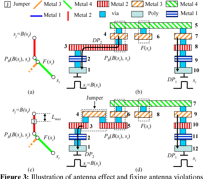 Figure 3 from Antenna Violation Avoidance/Fixing for X-clock routing | Semantic Scholar
 Antenna Effect in 16nm Technology Node
 Design rule checking - Wikipedia

 ⨘ } VLSI } 8 } Antenna Effects } - YouTube
 Antenna violations resolved using new method - EDN
 Discharge-path-based antenna effect detection and fixing for X-architecture clock tree - ScienceDirect
 Process Antenna Rule – sarvangsanghavi


Komentar
Posting Komentar